



Key takeaways
- Discovered Materials raised $9M in seed funding led by Lightspeed India Partners to build AI agents for chip design.
- The startup leverages AI agents to simulate, synthesize, and validate novel thermal management materials for GPUs.
- The company released Material Discovery Bench, an open-source tool evaluating frontier AI models on material science.
What happened
Discovered Materials, an artificial intelligence startup based in San Francisco, announced a $9 million seed funding round led by Lightspeed India Partners. The investment round featured participation from prominent venture firm Y Combinator, Peak XV Partners, and high-profile angel investors, including Paul Graham, Gokul Rajaram, and Thariq Shihipar.
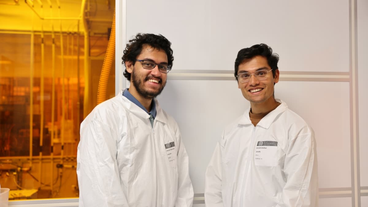
Founded by Indian Institute of Technology Madras graduates Advaith Sridhar and Akash Ramdas, the startup focuses on autonomous software agents designed to automate complex, multi-step workflows in materials science research.
The capital injection will be directed toward expanding the startup's core engineering team and physical laboratory infrastructure. Discovered Materials plans to scale its multi-agent platform, which conducts advanced computer simulations, chemical synthesis planning, and physical experimental validation.
During its recent stint in the Y Combinator accelerator program, the team successfully utilized its automated agents to design, synthesize, and evaluate novel thermal interface materials in just three months, matching performance metrics that traditionally require several years of research and development by legacy chemical enterprises.
Alongside the equity financing announcement, Discovered Materials unveiled Material Discovery Bench. This open-source evaluation benchmark is specifically designed to assess how well frontier large language models and autonomous agents can identify, reason about, and discover viable materials tailored for advanced semiconductor applications.
Why it matters
The rapid expansion of artificial intelligence workloads has escalated the severe thermal and power density challenges confronting modern semiconductor architectures. High-performance graphics processing units now routinely endure extreme thermal loads reaching approximately 140 watts per square centimeter, a metric projected to surge higher as model training requirements grow.
Without significant breakthroughs in heat dissipation and thermal generation reduction, next-generation chip designs, such as dense 3D wafer stacking where logic and memory components are closely integrated, will hit severe thermodynamic limits.
Traditional methods for discovering and commercializing new materials—often termed the "lab-to-fab" pipeline—are notoriously slow, capital-intensive, and prone to high failure rates. Developing a single viable compound and integrating it into commercial semiconductor manufacturing facilities typically demands hundreds of millions of dollars and takes over a decade.
By utilizing domain-specific autonomous AI agents to manage physical and digital research workflows, Discovered Materials demonstrates how agentic AI can radically compress scientific discovery cycles and lower the cost structure of deep-tech hardware innovations.
What to watch
Industry observers and chip designers should track how effectively Discovered Materials transitions its laboratory findings into real-world fabrication plants, as well as how major frontier AI laboratories perform on the newly released Material Discovery Bench benchmark.
As investor capital flows heavily into domain-specific agentic platforms across vertical industries, the ability of AI agents to reliably interface with physical laboratory equipment and solve core thermodynamic bottlenecks in hardware will serve as a crucial test case for the broader agentic AI ecosystem.